Physical Effects/Overview of Mechanism:
Fast Marching Methodology:
Sample Simulations:
In the figure on the left, we use a model Gaussian function which is radially symmetric of the form
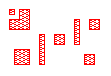
In the figure on the right, we use a masking pattern given in the figure, using an I-line stepper, numerical aperture 0.6. The rate function is calculated using the three-dimensional exposure and post-exposure bake modules of TMA's Depict 4.0, and this is coupled to our fast marching level set method.
 (72K)
(72K)
|
 (286K)
|
| Evolution of single contact hole | Evolution under mask pattern |
| Model Gaussian rate function | Rate calculated using TMA's Depict |